

Light Detection and Ranging (LIDAR) Photonics
If you have a project involving LIDAR photonics, we can help you with the engineering and design by providing Ansys simulation software, training, and support as well as our consulting services.
Introduction:
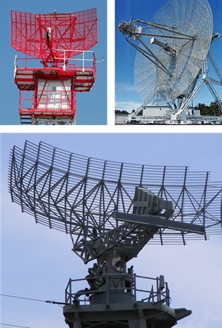
Light Detection and Ranging (LIDAR) is a technology based on the well known RADAR technology based on radio waves in use since the early 20th century to detect distant objects. Figure 1 shows examples of some of the RADARS in use today. One of the limitations of using a single antenna RADAR was since it radiates power in all the directions, it required a lot of power to detect far away objects. Also the directional information obtained was limited. An innovation which helped solve this problem was to use an array of antennas to create a directional beam which could be then used to probe a particular direction. By tuning the relative optical phases between the antennas the beam could be scanned in different directions. Fig. 2(a) shows a picture of an RADAR array. Figure 2(b) shows the schematic of a typical antenna array and how different phases may be tuned to sweep and scan the beam in different directions. In case of LIDAR, optical frequencies are used instead of radio frequencies.
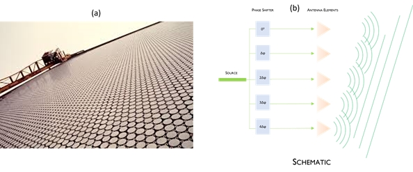
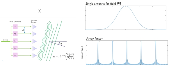
Fig. 3(a) shows how the beam angle α can be changed by changing the relative phase shift Δϕ between the different array elements as well as the wavelength λ. This allows the beam to be steered in different directions. Fig. 3(b) shows the single antenna field as well the effect of an array which is called as the array factor (AF). The output of an array is given by the product of a single antenna field multiplied by AF. More concretely the output field profile is given by:
![]() where U(θ,ϕ) is the field profile of a single antenna, N is the number of antennas, k is the wave vector, wi is the complex factor for array element i, ri is the position vector of antenna element i. The parameter wi can be tuned to steer the beam in any direction. For example to steer the beam at 45°, the vector w=[w1,w2,…] can be set to:
where U(θ,ϕ) is the field profile of a single antenna, N is the number of antennas, k is the wave vector, wi is the complex factor for array element i, ri is the position vector of antenna element i. The parameter wi can be tuned to steer the beam in any direction. For example to steer the beam at 45°, the vector w=[w1,w2,…] can be set to: ![]()
II. LIDAR design using Lumerical: Various packages in Lumerical can be used to design a LIDAR system. Here we show how Lumerical can be used to design an integrated Silicon based LIDAR system. In particular, corrugated waveguides can be used as antennas. The pitch of the corrugation is chosen so that the Bragg reflected light is scattered to free space. This happens when the corrugation pitch Λ is given by:
![]()
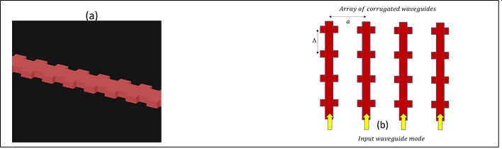
where λ0 is wavelength of the scattered light and neff is the effective index of the waveguide. Practically the pitch Λ is chosen so that the scattered light is not emitted normal to the antenna plane, but at a slight angle. This is done to avoid interference effects inside the chip slab. Fig. 4(a) shows the schematic of a corrugated waveguide. Multiple such waveguides can be arranged to create an antenna array which is shown in Fig. 4(b).
LIDAR design using Lumerical involves the following steps:
- MODE analysis to calculate the n_eff of the waveguide mode.
- Choosing optimum antenna separation so that there is minimum coupling between adjacent antennas.
- 3d FDTD simulation to calculate bandgap region.
- Far field analysis to calculate far-field profile of a single antenna.
- Array factor multiplication to see beam steering.
Lumerical MODE solutions can be used to calculate the effective refractive index of a waveguide mode. MODE uses Finite Difference Eigenmode solver which solves the Maxwell’s equations on a cross-section of the waveguide. Since we are using a corrugated waveguide with 2 different cross-sections, we can perform a sweep to calculate the neff at different cross-section widths.
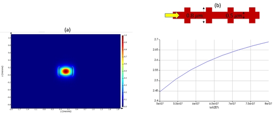
Fig. 5(a) shows the mode profile of the fundamental mode of a waveguide calculated using MODE. Fig. 5(b) shows the schematic of a corrugated waveguide with 2 different widths used to design antennas in the 1.5-1.6 μm wavelengths. Fig. 5(b) also shows the plot results of sweep for different waveguide widths and shows how the effective refractive index of the fundamental waveguide mode changes. For a corrugated waveguide with 2 different waveguide widths, a good estimate of the mode refractive index is the average of the effective refractive indices of the 2 waveguide widths. This can then be used to set the parameter Λ.
In the beam steering analysis we discussed before, it is important that there is no light coupling between different antenna elements. This means the array elements have a certain minimum separation between them. MODE can be used to find this separation. FDE can also be used to find the effective refractive index of a two coupled waveguides. This can be used to calculate what is the length needed before light from one waveguide couples to the other waveguide. Since in a corrugated waveguide we are dealing with 2 different cross-sections, this analysis has to performed twice for the 2 widths. This is illustrated in Fig. 6(a).
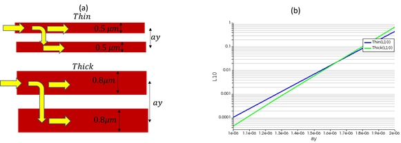
Fig. 6(b) shows the approximate length for 10% of the light to couple from one waveguide to the other for different values of ay. Based on this analysis we can chose separation to be close to 1.5 μm with around 6-7 mm needed for 10% light coupling, which is several wavelengths long.
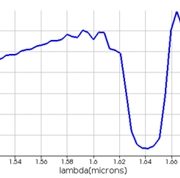
Figure 7
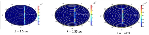
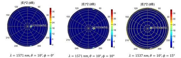
Next we use Lumerical FDTD to first calculate the band-gap of single corrugated antenna. This can be seen in Fig. 7. This plot shows the transmission for different wavelengths through the corrugated waveguide. We see that for wavelengths of interest from 1.5-1.6 μm, the transmission is between 40%-60%. We also see the band-gap region in the form of a transmission dip. Next we use the fields obtained using FDTD simulations to calculate the far-field using a far-field transmission. Fig. 8 shows how the field maxima can be steered in θ,ϕ space by changing λ. The contours correspond to ϕ and θ increases in the radial direction.
The far fields of a single antenna can be used to calculate the far-field of an antenna array. We can choose a certain direction for the beam in terms of θ,ϕ and the corresponding λ and the required phase delay Δϕ can be calculated.
We can see this beam steering in Fig. 9.
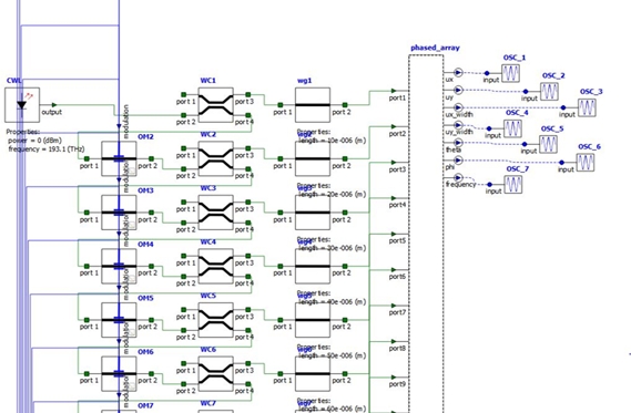
Additionally, we can use INTERCONNECT to perform system level simulations. This allows us to integrate multiple components and simulate an actual experiment. INTERCONNECT has an extensive internal library of standard components like continuous wave laser, waveguide couplers and modulators. In addition, INTERCONNECT also allows us to integrate a customized component. For example, we can integrate a phased array which we just designed using MODE and FDTD. This allows us to integrate optical, thermal and electrical elements together. Fig. 10 shows the layout of various components in an example of INTERCONNECT simulations. We can see different components like CWL (Continuous wave laser) source, WC (waveguide couplers) , wg (waveguides).
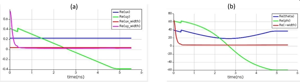
In addition, we can use can OM (optical modulator) to sweep various values of delays by changing applied voltages to the OM. At the output we can choose to read out various parameter values. For example, we can sweep various values of voltages to the OM and observe how beam angles θ,ϕ change. This can be seen in Fig. 11. We also see how the beam width changes as we change the applied voltage with time. Initially we see that the beam width is high because the beam is not well-formed.
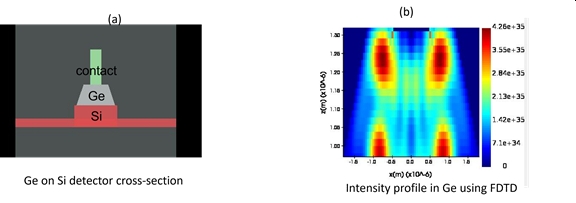
In addition to antenna and array design, we can also use Lumerical to design active elements like detectors which are vital components of a LIDAR system. Here we show how an integrated waveguide-coupled Germanium based avalanche photo-detector on silicon. These devices because of their high gain (reaching a few hundred) can be used to detect very weak signals. A cross-sectional schematic of such a detector can be seen in Fig. 12(a). Here we see a Si waveguide with a layer of Ge with a conducting contact on top. We first perform an FDTD simulation to calculate the field profile in the Ge region. This can be then used to calculate the carrier concentration in the Ge region which is proportional to field intensity. This can be seen in Fig. 12(b).
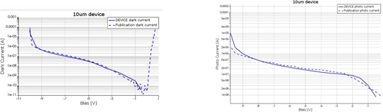
The generated charge carriers can be then swept through the contact into an external circuit using an electrical bias. We can then use Lumerical CHARGE to calculate the dark current and photocurrent of the Ge photodiode using drift diffusion equations and Poisson equations for electrons and holes for different values of applied bias voltages. This can be seen in Fig. 13. We see that it compares well with observed diode characteristics.
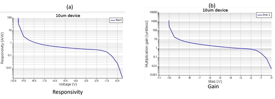
This data can be used to calculate characteristics like Gain and Responsivity for the device. The responsivity is defined as:
![]()
where Ilight and Idark are the currents in the presence and absence of light respectively. Pin is the input optical power. To find gain, we first calculate the voltage Vug for which the second derivative:
![]()
The multiplication gain at a certain voltage V is then obtained by taking the ratio:
![]()
We see the results plotted in Fig. 14.
Because of their high gains, APDs can be used to perform high speed data transmission (GHZ) speeds when biased near the breakdown region. At very high gains, typically diodes suffer from bandwidth degradation and are slower. However at moderate gains we can obtain high bit rates with low distortion. Typically these are studied using eye-diagrams as shown in Fig. 15 which were obtained using INTERCONNECT for different values of APD multiplication gain.
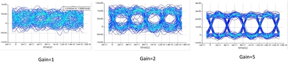
We see that the as the value of gain increases the eye opens up more and more, basically signifying an improvement in the signal to noise ratio and the fact that 0-bit and the 1-bit can be more easily distinguished.
If you have a project involving LIDAR photonics, we can help you with the engineering and design by providing Ansys simulation software, training, and support as well as our consulting services.
[maxbutton id=”3″ url=”/contact-us/” text=”Contact Us” ]