Ozen Ansys HFSS PCIe Compliance Template
Take the Pain Out of PCIe Compliance
Our Ansys HFSS PCIe Compliance Template simplifies this process. It’s a full-featured solution designed to validate designs and ensure compliance with PCIe standards, from Gen 1 to Gen 7. With this template, you can quickly simulate and analyze your designs, saving time and reducing errors.
Download PCIe1 and PCIe2 Compliance Templates
Please complete for the form below to get your free PCIe1 & PCIe2 compliance template download. To purchase the complate PCIe Gen 1 to Gen 7 template set, click here.
This download link will expire in 5 minutes:
Click here to download.
This PCI Express (PCIe) compliance template Software License Agreement (this “Agreement”) is a binding contract between Ozen Engineering Inc. (“Vendor”) and the individual or type of Person intending to download, install or otherwise use the Software hereinafter referred to as “Licensee”.
VENDOR PROVIDES THE SOFTWARE SOLELY ON THE TERMS AND CONDITIONS SET FORTH IN THIS AGREEMENT AND ON THE CONDITION THAT LICENSEE ACCEPTS AND COMPLIES WITH THEM. BY CLICKING THE “ACCEPT” BUTTON BELOW AND/OR BY DOWNLOADING INSTALLING OR OTHERWISE USING THE SOFTWARE LICENSEE (A) ACCEPTS THIS AGREEMENT AND AGREES THAT LICENSEE IS LEGALLY BOUND BY ITS TERMS; AND (B) REPRESENTS AND WARRANTS THAT: (I) IF AN INDIVIDUAL LICENSEE IS 18 YEARS OF AGE OR OLDER; AND (II) LICENSEE HAS THE RIGHT POWER AND AUTHORITY TO ENTER INTO THIS AGREEMENT AND BIND LICENSEE TO ITS TERMS. IF LICENSEE DOES NOT AGREE TO THE TERMS OF THIS AGREEMENT VENDOR WILL NOT AND DOES NOT LICENSE THE SOFTWARE TO LICENSEE AND LICENSEE MUST NOT DOWNLOAD INSTALL OR USE THE SOFTWARE OR DOCUMENTATION.
The Vendor wishes to license computer software to the Licensee and the Licensee desires to purchase the software license under the terms and conditions stated below.
IN CONSIDERATION OF the provisions contained in this Agreement and for other good and valuable consideration, the receipt and sufficiency of which is acknowledged, the parties agree as follows:
Under this Agreement, the Vendor grants to the Licensee a non-exclusive and non-transferable license (the "License") to use _ “PCI Express (PCIe) compliance template” __ (the "Software").
"Software" includes the project archive of the template and any other files that may accompany the product.
Title, copyright, intellectual property rights, and distribution rights of the Software remain exclusively with the Vendor. Intellectual property rights include the look and feel of the Software. This Agreement constitutes a license for use only and is not in any way a transfer of ownership rights to the Software.
The Software may be loaded onto no more than one computer. A single copy may be made for backup purposes only.
The rights and obligations of this Agreement are personal rights granted to the Licensee only. The Licensee may not transfer or assign any of the rights or obligations granted under this Agreement to any other person or legal entity. The Licensee may not make available the Software for use by one or more third parties.
The Software may not be modified, reverse-engineered, or de-compiled in any manner through current or future available technologies.
Failure to comply with any of the terms under the License section will be considered a material breach of this Agreement.
The Software is provided by the Vendor and accepted by the Licensee "as is". Liability of the Vendor will be limited to a maximum of the original purchase price of the Software. The Vendor will not be liable for any general, special, incidental, or consequential damages including but not limited to loss of production, loss of profits, loss of revenue, loss of data, or any other business or economic disadvantage suffered by the Licensee arising out of the use or failure to use the Software.
The Vendor makes no warranty expressed or implied regarding the fitness of the Software for a particular purpose or that the Software will be suitable or appropriate for the specific requirements of the Licensee.
The Vendor does not warrant that use of the Software will be uninterrupted or error-free. The Licensee accepts that software in general is prone to bugs and flaws within an acceptable level as determined in the industry.
The Vendor warrants and represents that it is the copyright holder of the Software. The Vendor warrants and represents that granting the license to use this Software is not in violation of any other agreement, copyright or applicable statute.
All terms, conditions, and obligations of this Agreement will be deemed to be accepted by the Licensee ("Acceptance") upon execution of this Agreement.
No user support or maintenance is provided as part of this Agreement.
The term of this Agreement will begin on Acceptance and is perpetual.
This Agreement will be terminated and the License forfeited where the Licensee has failed to comply with any of the terms of this Agreement or is in breach of this Agreement. On termination of this Agreement for any reason, the Licensee will promptly destroy the Software or return the Software to the Vendor.
The Vendor will be free of liability to the Licensee where the Vendor is prevented from executing its obligations under this Agreement in whole or in part due to Force Majeure such as earthquake, typhoon, flood, fire, and war or any other unforeseen and uncontrollable event where the Vendor has taken any and all appropriate action to mitigate such an event.
The Parties to this Agreement submit to the jurisdiction of the courts of the State of California for the enforcement of this Agreement or any arbitration award or decision arising from this Agreement. This Agreement will be enforced or construed according to the laws of the State of California.
This Agreement can only be modified in writing signed by both the Vendor and the Licensee.
This Agreement does not create or imply any relationship in agency or partnership between the Vendor and the Licensee.
Headings are inserted for the convenience of the parties only and are not to be considered when interpreting this Agreement. Words in the singular mean and include the plural and vice versa. Words in the masculine gender include the feminine gender and vice versa. Words in the neuter gender include the masculine gender and the feminine gender and vice versa.
If any term, covenant, condition, or provision of this Agreement is held by a court of competent jurisdiction to be invalid, void, or unenforceable, it is the parties' intent that such provision be reduced in scope by the court only to the extent deemed necessary by that court to render the provision reasonable and enforceable, and the remainder of the provisions of this Agreement will in no way be affected, impaired, or invalidated as a result.
This Agreement contains the entire agreement between the parties. All understandings have been included in this Agreement. Representations which may have been made by any party to this Agreement may in some way be inconsistent with this final written Agreement. All such statements are declared to be of no value in this Agreement. Only the written terms of this Agreement will bind the parties.
This Agreement and the terms and conditions contained in this Agreement apply to and are binding upon the Vendor's successors and assigns.
Key Features
- Broad PCIe Generation Support: Compatible with PCIe Gen 1 through Gen 7.
- Comprehensive Eye Diagram Analysis: Determines eye width and height for 1e-12 BER, ensuring your design meets critical specifications.
- Detailed Bathtub Curves: Evaluate signal integrity and determine eye height at various BER levels.
- Advanced Signature Analysis: Identifies bad transitions, impedance changes, crosstalk, jitter, and other signal irregularities.
- Customizable Equalization Parameters: Adjust or remove equalization to test line performance.
- Pre and Post Processing Included: Focus on design, not the setup.

PCIe Template covers PCIe 1-7 standards
Why Choose Our Template?
- Ease of Use: Only requires S-parameters of a full/partial link.
- Enhanced Visualization: Clear, easy-to-understand plots and graphs.
- User-Friendly Tools: Includes HFSS for studying eye width and signal under traces.
- Comprehensive Support: Covers return loss, differential return loss, common mode return loss, and more.
- Fast, Reliable Analysis: Detect and resolve design issues swiftly.

Detailed Technical Capabilities
The template is available for purchase by Ansys users to validate designs and ensure compliance with the PCIe standard. The template includes a built-in ready-to-use workspace, with no need for standards expertise.
Key Inclusions:
- Eye Diagram Analysis: Essential for determining if your PCIe signals meet the required standards for BER. The template uses the bathtub curve to determine the eye width and height at 1e-12 BER. Eye diagrams are crucial in identifying signal integrity issues.
- Bathtub Curve Analysis: Provides detailed bathtub curves that evaluate signal integrity and eye height at various BER levels, helping ensure your design meets critical specifications. Bathtub curves give a comprehensive view of signal performance over time.
- Signature Analysis: Helps identify and troubleshoot bad transitions, impedance changes, crosstalk, jitter, and other irregular signal phenomena. Each signature has a meaning and can highlight specific issues such as impedance mismatches or excessive jitter.
- Equalization Parameters: These parameters are crucial for ensuring the PCIe lines maintain sufficient bandwidth. The template allows you to modify or remove equalization to study its effects. The ability to test with or without equalization helps in understanding the performance limits.
- S-Parameters: The only input required is the S-parameters of a full/partial link. This significantly simplifies the setup process, enabling quicker analysis. The S-parameters define the electrical behavior of your PCIe channels.
- Return Loss Analysis: PCIe specifies return loss, differential return loss, and common mode return loss. Each standard has its specifications extended to a frequency point. The template provides detailed plots for these parameters, helping ensure your designs meet all necessary standards.
-
Pre-Configured Test Setups: Multiple pre-configured test setups are embedded within the template, covering a range of PCIe compliance requirements. This includes eye diagrams, return loss, differential return loss, and common mode return loss, with all parameters and limits predefined for ease of use.
-
Automated Compliance Checks: The template automates various compliance checks, such as validating signal integrity, ensuring compliance with PCIe standards, and identifying any design flaws early in the process.
-
Comprehensive Simulation Capabilities: Supports advanced simulations including crosstalk analysis, jitter impact analysis, and power integrity studies. This helps in understanding the interplay between different signal integrity issues and how they affect overall performance.
- Data Visualization: Advanced data visualization tools within HFSS allow for clear interpretation of results, making it easier to pinpoint areas of concern and optimize your design for better performance.
- Integration with Other Tools: Seamlessly integrates with other Ansys tools, allowing for a holistic approach to design and analysis. This includes integration with SIwave for power integrity and EM simulation and with DesignerSI for system-level analysis.
- Documentation and Reporting: The template includes features for generating comprehensive reports and documentation, which can be customized to include all relevant data and analysis results. This ensures all stakeholders have access to detailed insights into the design process.
- Return Loss Analysis: PCIe specifies return loss, differential return loss, and common mode return loss. Each standard has its specifications extended to a frequency point. The template provides detailed plots for these parameters, helping ensure your designs meet all necessary standards.
- Group Delay Analysis: Understand the delay between lines by calculating the skew based on the group delay of the differential mode. This is crucial for maintaining signal integrity across the PCB.
- Advanced HFSS Capabilities: Includes options for adding random/continuous/discontinuous jitter or noise and supports advanced eye width analysis. Users can study the eye width of the signal under traces and make adjustments as needed.
Learn More
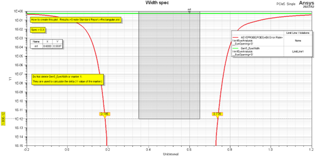

Bathtub with eye-width spec predefined.

Eye diagram with eye-height spec predefined.

Eye diagram with eye-height spec predefined.

Eye diagram with parameters: no-equalization/partial equalization/full equalization

Stressed eye analysis and ey-width verification against the PCE spec

Differential mode return loss specifications

Common mode return loss specifications

Interpair skew between two PCIe lines

TDR results of the line to identify impedance/transition irregularities.
